


Showing posts with label Electronics. Show all posts
Showing posts with label Electronics. Show all posts
Posted on
Friday, 9 December 2011

Read More
A 3 bit microprocessor can be designed using a 89C51 micro controller. This code for the program is written in the C language. The
code is then loaded into the "Keil uVision 2" Software and a hex file is made
through the software. The Hex File is then burned on to the micro controller
using a micro controller burner. The circuit diagram is shown below and "Proteus"
was used to simulate the software. The Hex file can be directly loaded into the Micro controller using the Proteus Software.
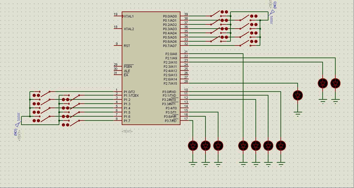
Working of the Project:
Setting numbers as Input:
The project makes use of the basic
programming techniques using the C language. First of all basic programs are
made as functions like addition function, subtraction function, multiplication function
and so on. Then the number is input
through the Port 0 of the micro controller. The input is always a binary
number.
Selecting an Operation:
After the two inputs are set onto
the switches then the operation switch is turned on. Operations are defined on the Port 1 of the micro controller. As it
is a 3 bit microprocessor so the total number of operations would be 23=8.
So the whole Port 1 is for operations. The operations include the basic
mathematical and logical operations. Selection of two operations at the same
time will generate an error and the error bit (Port 2 Pin 7) will turn on
indicating the error.
Displaying an Output:
The output is displayed in
the output registers. As it is a 3 bit microprocessor so all the registers will
be of 3 bits, so when the output of addition is increases than 7 or can’t be
displayed in the three bits the overflow bit (Port 2 Pin 0) is turned on
indicating the overflow.
In case
of multiplication, if the input goes higher than 3 bits then the second
register is used to display the remaining bits of the solution. In this way the
basic architecture of the computer is followed in the microprocessor.
Flag Register:
Flag register is again of
three bits. It contains 3 flag indicators that are zero flag, overflow flag and
the sign flag. The zero flag turns on to indicate a result equal to zero. The
overflow flag turn to indicate the overflow of the 1st output
register. The sign flag indicates a negative result.
Error Bit:
Error
bit is used to indicate an error either in the input port or the operations
port. In case of two operations being turned on at the same time, the error bit
turns on. Similarly when there is division by zero, the error bit indicates the
error.
Note:
This project was implemented and is found fully working. The
hex file and the C file are attached for the help. Furthermore the Proteus design
is also attached along with the files.
Posted on
Thursday, 8 December 2011
Read More
Mixer is a non-linear circuit that combines two signals in such a way to produce the sum and difference of the two input frequencies at the output.


COMPONENTS:-
C1 = 0.1uF
C2 = 0.1uF
C3 = 0.1uF
R1 = R2 = 10kOhm
R3 = R4 = 100kOhm
R5 = 6.8kOhm
The design and simulation was carried out in ADS software. And the circuit is like this:-

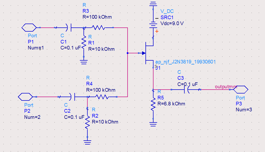
The mixer is implemented by an NPN transistor 2N3904.
The circuit used was basically for audio mixing, it had an input from the triangular wave generator and the noise generator. And it is passsed through the audio mixer to form the wave.
The practical waveform was like dis:-

While the waveform from simulation in ADS was like this:-

Posted on
Monday, 5 December 2011


Read More

The robot project works with two motors for driving the rear
wheels while the front wheels are free.
It uses 4 infra red sensors for detecting the line that it
has to follow. It can be either a black line on white background or a white
line on black background.
AT89C2051 microcontroller is used in the project for instructing the robot to move according to
the sensors input. The motor driving circuit is made with L293D, which is an
H-bridge IC. It can control the two motors simultaneously.
The code is written in C and is a fully functional code.
Care must be taken while choosing the motors. It should be a
high torque motor so that it can take the weight of your robot. Otherwise the
wheels would work fine while in the air but would not move once the robot is
set down.
The sensor circuits as well as the control circuit is given
below and the C code can be downloaded as a word file.
Control circuit:-

Sensors circuit:-
These sensor circuits need to be attatched at the points labeled as sensors in the main figure.

Position of Sensors:-

C code:-
Posted on
Saturday, 3 December 2011

The basic operation of the circuit is based on impedance matching and then amplifying the signal to give it to the output. Two normal speakers can be used both as the input and the output devices. The first stage which is at BC109C receives the signal in the common base configuration. It gives a good voltage gain and low input impedance which is used for impedance matching with the 8ohms speaker.
Self DC bias is used allowing variations in the transistor’s current gain.
The signal is then filtered for any DC part that may be present, through the capacitor. Thus a pure AC audio signal is sent to the 2nd part of the circuit which is the audio amplifier booster.
A constant Vcc is provided to this circuit, the two diodes check the backward flow of current. The signal is amplified on the 2nd stage through 2 transistors in cascade and later the signal is purified through a capacitor and sent to the output speaker. The basic function of the amplifier is to boost the voltage gain of the circuit and than provide it to the output speaker.
The circuit i used instead of LM386 is:-

OUTPUT ANALYSIS
The output analysis of the circuit tells that its providing 2 watts gain to the speaker so that the voice is audible. If the gain of the amplifier exceed s above the limit than the output signal is clipped off.
Read More

The basic operation of the circuit is based on impedance matching and then amplifying the signal to give it to the output. Two normal speakers can be used both as the input and the output devices. The first stage which is at BC109C receives the signal in the common base configuration. It gives a good voltage gain and low input impedance which is used for impedance matching with the 8ohms speaker.
Self DC bias is used allowing variations in the transistor’s current gain.
The signal is then filtered for any DC part that may be present, through the capacitor. Thus a pure AC audio signal is sent to the 2nd part of the circuit which is the audio amplifier booster.
A constant Vcc is provided to this circuit, the two diodes check the backward flow of current. The signal is amplified on the 2nd stage through 2 transistors in cascade and later the signal is purified through a capacitor and sent to the output speaker. The basic function of the amplifier is to boost the voltage gain of the circuit and than provide it to the output speaker.
The circuit i used instead of LM386 is:-

OUTPUT ANALYSIS
The output analysis of the circuit tells that its providing 2 watts gain to the speaker so that the voice is audible. If the gain of the amplifier exceed s above the limit than the output signal is clipped off.
Posted on
Friday, 2 December 2011
Read More
Circuit Diagram:

Components:


Components:
·
2x LM 741 IC’s
·
20kΩ Resistor
·
5kΩ Resistor
·
10kΩ Resistor
·
1.1uF Capacitor
Working:
Assemble the components as shown in the circuit diagram
above. In the above diagram the capacitor C1 acts as a integrator and
integrates the square input into a triangular wave. In this way a triangular
wave is generated.
Results:
Result of the above circuit diagram is a perfect triangular
wave.
Posted on

Abstract
This paper begins with background information. First, introductory
Topics on the basic principles of amplifiers are presented, including
the ideal op amp model, next the design, layout, simulation and noise theory of Operational Amplifier (Op-Amp) structures. Emphasis has been placed on the noise properties of the Op-Amp performance. The OP-Amp noise types and characteristics. Our results show that Experimental testing needs to be carried out for further evaluations.
History:
1941: First (vacuum tube) op-amp
Let's go back in time a bit and see how this device was developed. The term "operational amplifier" goes all the way back to about 1943 where this name was mentioned in a paper written by John R. Ragazzinni with the title "Analysis of Problems in Dynamics" and also covered the work of technical aid George A. Philbrick.
Today, and since that month in 1976, the types of op amps have increased almost daily. An op-amp, defined as a general-purpose, DC-coupled, high gain, inverting feedback amplifier, was first found in US Patent 2,401,779 "Summing Amplifier" filed by Karl D. Swartzel Jr. of Bell labs in 1941. This design used three vacuum tubes to achieve a gain of 90dB (decibells) and operated on voltage rails of ±350V. It had a single inverting input rather than differential inverting and non-inverting inputs, as are common in today's op-amps.
INTRODUCTION
What exactly is an OPerational AMPlifier? Let's define what that component is and look at the parameters of this amazing device. An operational amplifier IC is a solidstate integrated circuit that uses external feedback to control its functions. It is one of the most versatile devices in all of electronics. The term 'op-amp' was originally used to describe a chain of high performance DC amplifiers that was used as a basis for the analog type computers of long ago. The very high gain op-amp IC's our days uses external feedback networks to control responses. The op-amp without any external devices is called 'open-loop' mode, refering actually to the so-called 'ideal' operational amplifier with infinite open-loop gain, input resistance, bandwidth and a zero output resistance. However, in practice no op-amp can meet these ideal characteristics.
EXPLANATION
An operational amplifier is a differential input, single-ended output amplifier, as shown symbolically in Figure 1-1. This device is an amplifier intended for use with external feedback elements, where these elements determine the resultant function, or operation. This gives rise to the name “operational amplifier,” denoting an amplifier that, by virtue of different feedback hookups, can perform a variety of operations.
We now enjoy a variety of op amps that will provide the user essentially with anything s/he needs, such as high common-mode rejection, low-input current frequency compensation, CMOS, and short-circuit protection. All a designer has to do is expressing his needs and is then supplied with the correct type. Op-Amps are continually being improved, especially in the low noise areas.
Ideal Op Amp Attributes
An ideal op amp has infinite gain for differential input signals. In practice, real devices will have quite high gain (also called open-loop gain) but this gain may not necessarily be precisely known. In terms of specifications, gain is measured in terms of VOUT/VIN, and is given in V/V, the dimensionless numeric gain. More often, however, gain is expressed in decibel terms (dB), which is mathematically dB = 20 • log (numeric gain).
Also, an ideal op amp has zero gain for signals common to both inputs, that is, common-mode (CM) signals.
Or, stated in terms of the rejection for these common-mode signals, an ideal op amp has infinite CM rejection (CMR). In practice, real op amps can have CMR specifications of up to 130 dB for precision devices, or as low as 60 dB–70 dB for some high speed devices.
The ideal op amp also has zero offset voltage (VOS = 0), and draws zero bias current (IB = 0) at both inputs. Within real devices, actual offset voltages can be as low as 1 pV or less, or as high as several mV. Bias currents can be as low as a few fA, or as high as several ìA. This extremely wide range of specifications reflects the different input structures used within various devices.
The Noninverting Op Amp Stage
The op amp non-inverting gain stage, also known as a voltage follower with gain, or simply voltage follower,
Transfer expression of the network is defined as seen from the top of RF to the output across RG as β. This usage is a general feedback network transfer term, not to be confused with bipolar transistor forward gain. β can be expressed mathematically.
So, the feedback network returns a fraction of Vout to the op amp (–) input. Considering the ideal principles of zero offset and infinite gain, this allows some deductions on gain to be made. The voltage at the (–) input is forced by the op amp’s feedback action to be equal to that seen at the (+) input, Vin. Given this relationship, it is relatively easy to work out the ideal gain of this stage, which in fact turns out to be simply the inverse of β. This is apparent from a comparison of Equations.
The Inverting Op Amp Stage
The op amp inverting gain stage, also known simply as the inverter, is shown in Figure 1-4. As can be noted by comparison of Figures 1-3 and 1-4, the inverter can be viewed as similar to a follower, but with a transposition of the input voltage Vin. In the inverter, the signal is applied to RG of the feedback network and the op amp (+) input is grounded.
For clarity, these expressions are again included in the figure. The major difference between this stage and the non-inverting counterpart is the input-to-output sign reversal, denoted by the minus sign in Eq. 1-5. Like the follower stage, applying ideal op amp principles and some basic algebra can derive the gain expression of Eq. 1-5.
The inverting configuration is also one of the more useful op amp stages. Unlike a non-inverting stage, however, the inverter presents a relatively low impedance input for Vin, i.e., the value of RG. This factor provides a finite load to the source. While the stage gain can in theory be adjusted over a wide range via RF and RG, there is a practical limitation imposed at high gain, when RG becomes relatively low. If RF is zero, the gain becomes zero. RF can also be made variable, in which case the gain is linearly variable over the dynamic range of the element used for RF. As with the follower gain stage, the gain is ratio dependent, and is relatively insensitive to the exact RF and RG values.
The inverter’s gain behavior, due to the principles of infinite op amp gain, zero input offset, and zero bias current, gives rise to an effective node of zero voltage at the (−) input. The input and feedback currents sum at this point, which logically results in the term summing point. It is also called a virtual ground, because of the fact it will be at the same potential as the grounded reference input.
A special gain case for the inverter occurs when RF = RG, which is also called a unity gain inverter. This form of inverter is commonly used for generating complementary VOUT signals, i.e., VOUT = −VIN. In such cases it is usually desirable to match RF to RG accurately, which can readily be done by using a wellspecified matched resistor pair.
A variation of the inverter is the inverting summer, a case similar to Figure 1-4, but with input resistors RG2, RG3, etc (not shown). For a summer individual input resistors are connected to additional sources VIN2, VIN3, and so forth, with their common node connected to the summing point. This confi guration, called a summing amplifier, allows linear input current summation in RF.3 VOUT is proportional to an inverse sum of input currents.
Noise Gain (NG)
The first aid to analyzing op amps circuits is to differentiate between noise gain and signal gain. We have already discussed the differences between noninverting and inverting stages as to their signal gains, which are summarized in Eqs. 1-2 and 1-4, respectively. But, as can be noticed from Figure 1-6, the difference between an inverting and noninverting stage can be as simple as where the reference ground is placed. For a ground at point G1, the stage is an inverter; conversely, if the ground is placed at point G2 (with no G1) the stage is noninverting.
Note, however, that in terms of the feedback path, there are no real differences. To make things more general, the resistive feedback components previously shown are replaced here with the more general symbols ZF and ZG, otherwise they function as before. The feedback attenuation, â, is the same for both the inverting and noninverting stages:
Noise gain can now be simply defined as: The inverse of the net feedback attenuation from the amplifier output to the feedback input. In other words, the inverse of the â network transfer function. This can ultimately be extended to include frequency dependence (covered later in this chapter). Noise gain can be abbreviated as NG.
As noted, the inverse of â is the ideal noninverting op amp stage gain. Including the effects of fi nite op amp gain, a modifi ed gain expression for the noninverting stage is:
Open-Loop Gain:
Lets have a look how the 'ideal' amplifier would look like in Fig. 5-1. The search for an ideal amplifier is, of course, a futile exercise. The characteristics of the operational amplifier are good enough, however, to allow us to treat it as ideal. Below are some amplifier properties that make this so. (Please realize that these ratings are next to impossible to achieve).
Op Amp Noise Theory and Applications
The purpose of op amp circuitry is the manipulation of the input signal in some fashion.
Unfortunately in the real world, the input signal has unwanted noise superimposed on it.
Noise is not something most designers get excited about. In fact, they probably wish the
whole topic would go away. It can, however, be a fascinating study by itself. A good understanding of the underlying principles can, in some cases, be used to reduce noise in the
design.
Noise is a purely random signal, the instantaneous value and/or phase of the waveform
cannot be predicted at any time. Noise can either be generated internally in the op amp,
from its associated passive components, or superimposed on the circuit by external sources.
Noise Floor
When all input sources are turned off and the output is properly terminated, there is a level
of noise called the noise floor that determines the smallest signal for which the circuit is
useful. The objective for the designer is to place the signals that the circuit processes
above the noise floor, but below the level where the signals will clip.
Signal-to-Noise Ratio
it is a ratio of signal voltage to noise voltage (hence the name signal-tonoise
ratio).
Types of Noise
There are five types of noise in op amps and associated circuitry:
1) Shot noise
2) Thermal noise
3) Flicker noise
4) Burst noise
5) Avalanche noise
Some or all of these noises may be present in a design, presenting a noise spectrum
unique to the system. It is not possible in most cases to separate the effects, but knowing
general causes may help the designer optimize the design, minimizing noise in a particular
bandwidth of interest. Proper design for low noise may involve a “balancing act” between
these sources of noise and external noise sources.
Noise Colors
While the noise types are interesting, real op amp noise will appear as the summation of
some or all of them. The various noise types themselves will be difficult to separate. Fortunately,
there is an alternative way to describe noise, which is called color. The colors of noise come from rough analogies to light, and refer to the frequency content. Many colors are used to describe noise, some of them having a relationship to the real world, and some of them more attuned to the field of psycho-acoustics.
White noise is in the middle of a spectrum that runs from purple to blue to white to pink
and red/brown. These colors correspond to powers of the frequency to which their spectrum
is proportional.
AMPLIFIER NOISE
Amplification of low level audio or RF signals is always accompanied by noise generated within the amplifier itself. The following article discusses the generation of this noise and some of the methods of assessing noise performance.
INTRODUCTION
One of the factors which governs the performance of any amplifier system is the noise in the system. Noise might be defined as signals in the system which are unwanted and which degrade the desired signal content in the system.
As far as the amplifier system is concerned, noise can be divided into noise it receives at its input and noise it generates itself. A good system is one in which the noise generated by the amplifier itself is small compared to noise from the incoming source. In a HF receiver, for example, atmospheric noise is high and it is not difficult to achieve this requirement. At VHF and UHF frequencies, atmospheric noise is low and performance is limited by the noise generated in the first stages of the radio receiver.
An operational amplifier, which is often called an op-amp, is a DC-coupled high-gain electronic voltage amplifier with differential inputs and, usually, a single output. Typically the output of the op-amp is controlled either by negative feedback, which largely determines the magnitude of its output voltage gain, or by positive feedback, which facilitates regenerative gain and oscillation. High input impedance at the input terminals (ideally infinite) and low output impedance (ideally zero) are important typical characteristics.
Op-amps are among the most widely used electronic devices today, being used in a vast array of consumer, industrial, and scientific devices. Many standard IC op-amps cost only a few cents in moderate production volume; however some integrated or hybrid operational amplifiers with special performance specifications may cost over $100 US in small quantities. Op-amps sometimes come in the form of macroscopic components (see photo), or as integrated circuit 'cells' or patterns that can be reprinted several times on one chip that is more complex, such as for a cell phone.
Modern designs are electronically more rugged than earlier implementations and some can sustain direct short circuits on their outputs without damage.
The op-amp is one type of differential amplifier. Other types of differential amplifier include the fully differential amplifier (similar to the op-amp, but with two outputs), the instrumentation amplifier (usually built from three op-amps), the isolation amplifier (similar to the instrumentation amplifier, but which works fine with common-mode voltages that would destroy an ordinary op-amp), and negative feedback amplifier (usually built from one or more op-amps and a resistive feedback network).
Read More

This paper begins with background information. First, introductory
Topics on the basic principles of amplifiers are presented, including
the ideal op amp model, next the design, layout, simulation and noise theory of Operational Amplifier (Op-Amp) structures. Emphasis has been placed on the noise properties of the Op-Amp performance. The OP-Amp noise types and characteristics. Our results show that Experimental testing needs to be carried out for further evaluations.
History:
1941: First (vacuum tube) op-amp
Let's go back in time a bit and see how this device was developed. The term "operational amplifier" goes all the way back to about 1943 where this name was mentioned in a paper written by John R. Ragazzinni with the title "Analysis of Problems in Dynamics" and also covered the work of technical aid George A. Philbrick.
Today, and since that month in 1976, the types of op amps have increased almost daily. An op-amp, defined as a general-purpose, DC-coupled, high gain, inverting feedback amplifier, was first found in US Patent 2,401,779 "Summing Amplifier" filed by Karl D. Swartzel Jr. of Bell labs in 1941. This design used three vacuum tubes to achieve a gain of 90dB (decibells) and operated on voltage rails of ±350V. It had a single inverting input rather than differential inverting and non-inverting inputs, as are common in today's op-amps.
INTRODUCTION
What exactly is an OPerational AMPlifier? Let's define what that component is and look at the parameters of this amazing device. An operational amplifier IC is a solidstate integrated circuit that uses external feedback to control its functions. It is one of the most versatile devices in all of electronics. The term 'op-amp' was originally used to describe a chain of high performance DC amplifiers that was used as a basis for the analog type computers of long ago. The very high gain op-amp IC's our days uses external feedback networks to control responses. The op-amp without any external devices is called 'open-loop' mode, refering actually to the so-called 'ideal' operational amplifier with infinite open-loop gain, input resistance, bandwidth and a zero output resistance. However, in practice no op-amp can meet these ideal characteristics.
EXPLANATION
An operational amplifier is a differential input, single-ended output amplifier, as shown symbolically in Figure 1-1. This device is an amplifier intended for use with external feedback elements, where these elements determine the resultant function, or operation. This gives rise to the name “operational amplifier,” denoting an amplifier that, by virtue of different feedback hookups, can perform a variety of operations.
We now enjoy a variety of op amps that will provide the user essentially with anything s/he needs, such as high common-mode rejection, low-input current frequency compensation, CMOS, and short-circuit protection. All a designer has to do is expressing his needs and is then supplied with the correct type. Op-Amps are continually being improved, especially in the low noise areas.
Ideal Op Amp Attributes
An ideal op amp has infinite gain for differential input signals. In practice, real devices will have quite high gain (also called open-loop gain) but this gain may not necessarily be precisely known. In terms of specifications, gain is measured in terms of VOUT/VIN, and is given in V/V, the dimensionless numeric gain. More often, however, gain is expressed in decibel terms (dB), which is mathematically dB = 20 • log (numeric gain).
Also, an ideal op amp has zero gain for signals common to both inputs, that is, common-mode (CM) signals.
Or, stated in terms of the rejection for these common-mode signals, an ideal op amp has infinite CM rejection (CMR). In practice, real op amps can have CMR specifications of up to 130 dB for precision devices, or as low as 60 dB–70 dB for some high speed devices.
The ideal op amp also has zero offset voltage (VOS = 0), and draws zero bias current (IB = 0) at both inputs. Within real devices, actual offset voltages can be as low as 1 pV or less, or as high as several mV. Bias currents can be as low as a few fA, or as high as several ìA. This extremely wide range of specifications reflects the different input structures used within various devices.
The Noninverting Op Amp Stage
The op amp non-inverting gain stage, also known as a voltage follower with gain, or simply voltage follower,
Transfer expression of the network is defined as seen from the top of RF to the output across RG as β. This usage is a general feedback network transfer term, not to be confused with bipolar transistor forward gain. β can be expressed mathematically.
So, the feedback network returns a fraction of Vout to the op amp (–) input. Considering the ideal principles of zero offset and infinite gain, this allows some deductions on gain to be made. The voltage at the (–) input is forced by the op amp’s feedback action to be equal to that seen at the (+) input, Vin. Given this relationship, it is relatively easy to work out the ideal gain of this stage, which in fact turns out to be simply the inverse of β. This is apparent from a comparison of Equations.
The Inverting Op Amp Stage
The op amp inverting gain stage, also known simply as the inverter, is shown in Figure 1-4. As can be noted by comparison of Figures 1-3 and 1-4, the inverter can be viewed as similar to a follower, but with a transposition of the input voltage Vin. In the inverter, the signal is applied to RG of the feedback network and the op amp (+) input is grounded.
For clarity, these expressions are again included in the figure. The major difference between this stage and the non-inverting counterpart is the input-to-output sign reversal, denoted by the minus sign in Eq. 1-5. Like the follower stage, applying ideal op amp principles and some basic algebra can derive the gain expression of Eq. 1-5.
The inverting configuration is also one of the more useful op amp stages. Unlike a non-inverting stage, however, the inverter presents a relatively low impedance input for Vin, i.e., the value of RG. This factor provides a finite load to the source. While the stage gain can in theory be adjusted over a wide range via RF and RG, there is a practical limitation imposed at high gain, when RG becomes relatively low. If RF is zero, the gain becomes zero. RF can also be made variable, in which case the gain is linearly variable over the dynamic range of the element used for RF. As with the follower gain stage, the gain is ratio dependent, and is relatively insensitive to the exact RF and RG values.
The inverter’s gain behavior, due to the principles of infinite op amp gain, zero input offset, and zero bias current, gives rise to an effective node of zero voltage at the (−) input. The input and feedback currents sum at this point, which logically results in the term summing point. It is also called a virtual ground, because of the fact it will be at the same potential as the grounded reference input.
A special gain case for the inverter occurs when RF = RG, which is also called a unity gain inverter. This form of inverter is commonly used for generating complementary VOUT signals, i.e., VOUT = −VIN. In such cases it is usually desirable to match RF to RG accurately, which can readily be done by using a wellspecified matched resistor pair.
A variation of the inverter is the inverting summer, a case similar to Figure 1-4, but with input resistors RG2, RG3, etc (not shown). For a summer individual input resistors are connected to additional sources VIN2, VIN3, and so forth, with their common node connected to the summing point. This confi guration, called a summing amplifier, allows linear input current summation in RF.3 VOUT is proportional to an inverse sum of input currents.
Noise Gain (NG)
The first aid to analyzing op amps circuits is to differentiate between noise gain and signal gain. We have already discussed the differences between noninverting and inverting stages as to their signal gains, which are summarized in Eqs. 1-2 and 1-4, respectively. But, as can be noticed from Figure 1-6, the difference between an inverting and noninverting stage can be as simple as where the reference ground is placed. For a ground at point G1, the stage is an inverter; conversely, if the ground is placed at point G2 (with no G1) the stage is noninverting.
Note, however, that in terms of the feedback path, there are no real differences. To make things more general, the resistive feedback components previously shown are replaced here with the more general symbols ZF and ZG, otherwise they function as before. The feedback attenuation, â, is the same for both the inverting and noninverting stages:
Noise gain can now be simply defined as: The inverse of the net feedback attenuation from the amplifier output to the feedback input. In other words, the inverse of the â network transfer function. This can ultimately be extended to include frequency dependence (covered later in this chapter). Noise gain can be abbreviated as NG.
As noted, the inverse of â is the ideal noninverting op amp stage gain. Including the effects of fi nite op amp gain, a modifi ed gain expression for the noninverting stage is:
Open-Loop Gain:
Lets have a look how the 'ideal' amplifier would look like in Fig. 5-1. The search for an ideal amplifier is, of course, a futile exercise. The characteristics of the operational amplifier are good enough, however, to allow us to treat it as ideal. Below are some amplifier properties that make this so. (Please realize that these ratings are next to impossible to achieve).
Op Amp Noise Theory and Applications
The purpose of op amp circuitry is the manipulation of the input signal in some fashion.
Unfortunately in the real world, the input signal has unwanted noise superimposed on it.
Noise is not something most designers get excited about. In fact, they probably wish the
whole topic would go away. It can, however, be a fascinating study by itself. A good understanding of the underlying principles can, in some cases, be used to reduce noise in the
design.
Noise is a purely random signal, the instantaneous value and/or phase of the waveform
cannot be predicted at any time. Noise can either be generated internally in the op amp,
from its associated passive components, or superimposed on the circuit by external sources.
Noise Floor
When all input sources are turned off and the output is properly terminated, there is a level
of noise called the noise floor that determines the smallest signal for which the circuit is
useful. The objective for the designer is to place the signals that the circuit processes
above the noise floor, but below the level where the signals will clip.
Signal-to-Noise Ratio
it is a ratio of signal voltage to noise voltage (hence the name signal-tonoise
ratio).
Types of Noise
There are five types of noise in op amps and associated circuitry:
1) Shot noise
2) Thermal noise
3) Flicker noise
4) Burst noise
5) Avalanche noise
Some or all of these noises may be present in a design, presenting a noise spectrum
unique to the system. It is not possible in most cases to separate the effects, but knowing
general causes may help the designer optimize the design, minimizing noise in a particular
bandwidth of interest. Proper design for low noise may involve a “balancing act” between
these sources of noise and external noise sources.
Noise Colors
While the noise types are interesting, real op amp noise will appear as the summation of
some or all of them. The various noise types themselves will be difficult to separate. Fortunately,
there is an alternative way to describe noise, which is called color. The colors of noise come from rough analogies to light, and refer to the frequency content. Many colors are used to describe noise, some of them having a relationship to the real world, and some of them more attuned to the field of psycho-acoustics.
White noise is in the middle of a spectrum that runs from purple to blue to white to pink
and red/brown. These colors correspond to powers of the frequency to which their spectrum
is proportional.
AMPLIFIER NOISE
Amplification of low level audio or RF signals is always accompanied by noise generated within the amplifier itself. The following article discusses the generation of this noise and some of the methods of assessing noise performance.
INTRODUCTION
One of the factors which governs the performance of any amplifier system is the noise in the system. Noise might be defined as signals in the system which are unwanted and which degrade the desired signal content in the system.
As far as the amplifier system is concerned, noise can be divided into noise it receives at its input and noise it generates itself. A good system is one in which the noise generated by the amplifier itself is small compared to noise from the incoming source. In a HF receiver, for example, atmospheric noise is high and it is not difficult to achieve this requirement. At VHF and UHF frequencies, atmospheric noise is low and performance is limited by the noise generated in the first stages of the radio receiver.
An operational amplifier, which is often called an op-amp, is a DC-coupled high-gain electronic voltage amplifier with differential inputs and, usually, a single output. Typically the output of the op-amp is controlled either by negative feedback, which largely determines the magnitude of its output voltage gain, or by positive feedback, which facilitates regenerative gain and oscillation. High input impedance at the input terminals (ideally infinite) and low output impedance (ideally zero) are important typical characteristics.
Op-amps are among the most widely used electronic devices today, being used in a vast array of consumer, industrial, and scientific devices. Many standard IC op-amps cost only a few cents in moderate production volume; however some integrated or hybrid operational amplifiers with special performance specifications may cost over $100 US in small quantities. Op-amps sometimes come in the form of macroscopic components (see photo), or as integrated circuit 'cells' or patterns that can be reprinted several times on one chip that is more complex, such as for a cell phone.
Modern designs are electronically more rugged than earlier implementations and some can sustain direct short circuits on their outputs without damage.
The op-amp is one type of differential amplifier. Other types of differential amplifier include the fully differential amplifier (similar to the op-amp, but with two outputs), the instrumentation amplifier (usually built from three op-amps), the isolation amplifier (similar to the instrumentation amplifier, but which works fine with common-mode voltages that would destroy an ordinary op-amp), and negative feedback amplifier (usually built from one or more op-amps and a resistive feedback network).
Posted on
Thursday, 1 December 2011

Abstract—the paper discusses that Solid-state relays (SSR) are able to perform many of the same tasks as electromechanical relay (EMRs). The main difference is that SSRs have no moving mechanical parts within it. SSRs use a control circuit and a separate circuit for switching the load. The relay is energized by a light-emitting diode. The types of SSR are photo-coupled SSR, transformer-coupled SSR, and hybrid SSR.
I-INTRODUCTION: Solid State Relays (SSRs) are switching devices consisting of electronic components. The term "Solid State" means that these relays do not incorporate any moving parts in the load switching circuit. Often, solid state relays are used where the circuit under control must be protected from the introduction of electrical noises. [1]
II-DEFINITION: A solid state relay (SSR) is an electronic switch, which contains no moving parts. Essentially, it is an electronic device that relies on the electrical, magnetic, and optical properties of semiconductors and electrical components to achieve its isolation and relay switching function [2].The SSR requires relatively low control circuit energy to switch the output state from OFF to ON, or vice versa. Since this control energy is very much lower than the output power controllable by the relay at full load, "power gain" in an SSR is substantial--frequently much higher. Being solid-state devices, there are no moving parts to wear out, and they are able to switch on and off much faster than any mechanical relay armature can move. There is no sparking between contacts, and no problems with contact corrosion. [3]
III-PRINCIPLE OF OPERATION: These active semiconductor devices use light instead of magnetism to actuate a switch. The light comes from an LED, or light emitting diode. When control power is applied to the device’s output, the light is turned on and shines across an open space. On the load side of this space, a part of the device senses the presence of the light, and triggers a solid state switch that either opens or closes the circuit under control. [4]
IV-TRIACS: A triac is an electronic component approximately equivalent to two silicon-controlled rectifiers joined in inverse parallel (paralleled but with the polarity reversed) and with their gates connected together. This results in a bidirectional electronic switch that can conduct current in either direction. The triac is ideal for switching resistive AC loads. [5]
SSRs use a control circuit and a separate circuit for switching the load. The output device (SCR, TRIAC, or transistor) is optically-coupled to an LED light source inside the relay. The relay is turned on by energizing this LED, usually with low-voltage DC power. When voltage is applied to the input of the SSR, the relay is energized by a light-emitting diode. The light from the diode is beamed into a light-sensitive semiconductor that, in the case of zero-voltage crossover relays, conditions the control circuit to turn on the output solid-state switch at the next zero-voltage crossover. In the case of nonzero-voltage crossover relays, the output solid-state switch is turned on at the precise voltage occurring at the time. Removal of the input power disables the control circuit and the solid-state switch is turned off when the load current passes through the zero point of its cycle. [6]
V-ADVANTAGES:
• When applied properly, Solid State Relays (SSRs) will last millions of cycles due to the fact that no mechanical devices are included in the load switching circuit. The user will experience no arcing problems, and operation will be trouble free, even in polluted environments (dust, gasses, etc.) SSRs are a faster alternative to electromechanical relays because their switching time is dependent on the time required to power the LED on and off - approximately 1 ms and 0.5 ms respectively. Because there are no mechanical parts, their life expectancy is higher than an electromechanical relay.
• One significant advantage of a solid-state SCR or TRIAC relay over an electromechanical device is its natural tendency to open the AC circuit only at a point of zero load current. Because SCR's and TRIAC's are thyristors, their inherent hysteresis maintains circuit continuity after the LED is de-energized until the AC current falls below a threshold value (the holding current). In practical terms what this means is the circuit will never be interrupted in the middle of a sine wave peak. Such untimely interruptions in a circuit containing substantial inductance would normally produce large voltage spikes due to the sudden magnetic field collapse around the inductance. This will not happen in a circuit broken by an SCR or TRIAC. This feature is called zero-crossover switching. [7]
• Additionally, SSRs are completely silent in their operation given their purely electronic nature.
• Increased lifetime due to the fact that there are no moving parts, and thus no wear
• Clean, bounce less operation
• Decreased electrical noise when switching
• Can be used in explosive environments where a spark must not be generated during turn-on
• Totally silent operation
• Smaller than a corresponding mechanical relay.
• Can continue to operate while subjected to severe vibration.
VI-DISADVANTAGES:
• One disadvantage of solid state relays is their tendency to fail "shorted" on their outputs, while electromechanical relay contacts tend to fail "open." In either case, it is possible for a relay to fail in the other mode, but these are the most common failures. Because a "fail-open" state is generally considered safer than a "fail-closed" state, electromechanical relays are still favored over their solid-state counterparts in many applications. [8]
• Fail short more easily than electro-mechanical relays
• Increased electrical noise when conducting
• Higher impedance when closed (-> heat production)
• Lower impedance when open
• Reverse leakage current when open (µA range)
• Possibility of false switching due to voltage transients
• Isolated bias supply required for gate charge circuit
• Higher Transient Reverse Recovery time (Trr) due to the presence of Body diode.
VII-TYPES OF SRR’s: It is convenient to classify SSR's by the nature of the input circuit, with particular reference to the means by which input-output isolation is achieved. Three major categories are recognized:
A-Reed-Relay-Coupled SSR’s in which the control signal is applied (directly, or through a preamplifier) to the coil of a reed relay. The closure of the reed switch then activates appropriate circuitry that triggers the thyristor switch. Clearly, the input-output isolation achieved is that of the reed relay, which is usually excellent.
B-Transformer-Coupled SSR’s in which the control signal is applied (through a DC-AC converter, if it is DC, or directly, if It is AC) to the primary of a small, low-power transformer, and the secondary voltage that results from the primary excitation is used (with or without rectification, amplification, or other modification) to trigger the thyristor switch. In this type, the degree of input-output isolation depends on the design of the transformer.
C-Photo-coupled SSR’s in which the control signal is applied to a light or infrared source (usually, a light-emitting diode, or LED), and the radiation from that source is detected in a photosensitive semi-conductor (i.e., a photosensitive diode, a photo-sensitive transistor, or a photo-sensitive thyristor). The output of the photo-sensitive device is then used to trigger (gate) the TRIAC or the SCR's that switch the load current. Clearly, the only significant “coupling path” between input and output is the beam of light or infrared radiation, and electrical isolation is excellent. These SSR's are also referred to as “optically coupled” or “photo-isolated. [9]
IX-Thermal considerations: one of the major considerations when using an SSR is properly managing the heat that is generated when switching currents higher than about 5 amperes (A). In this case, the base plate of the SSR should be mounted onto a good heat conductor, like aluminum, and used with a good thermal transfer medium like thermal grease or a heat transfer pad. Using this technique, the SSR case to heat sink thermal resistance is reduced to a negligible value of 0.1°C/W.
X-Load considerations: a leading cause of application issues with SSRs is improper heat sinking. Problems can also arise from operating conditions that specific loads impose upon an SSR. The surge characteristics of the load should be carefully considered when designing in a SSR as a switching solution.
XI-Resistive loads: Loads of constant values of resistance are the simplest application of SSRs. Proper thermal consideration, along with attention to the steady state current ratings, will result in trouble-free operation.
XII-DC loads: this type of load should be considered inductive, and a diode should be placed across the load to absorb any surges during turn-off.
XIII-Lamp loads: Incandescent lamp loads, though basically resistive, can present some challenges. Because the resistance of the cold filament is about 5 to 10 percent of the heated value, a large inrush current can occur. It is essential to verify that this inrush current is within the surge specifications of the SSR. One must also check that the lamp rating of the SSR is not exceeded. Due to the unusually low filament resistance at the time of turn-on, a zero-voltage turn-on characteristic is particularly desirable with incandescent lamps.
XIV-Capacitive loads: these types of loads can prove to be problematic because of their initial appearance as short circuits. High surge currents can occur while charging, limited only by circuit resistance. Caution must be used with low-impedance capacitive loads to verify that the di/dt capabilities are not exceeded. Zero-voltage turn-on is a particularly valuable means of limiting di/dt with capacitive loads.
XV-Motors and solenoids: Motor and solenoid loads can create challenges for reliable SSR functionality. Solenoids have high initial surge currents because their stationary impedance is very low. Motors also frequently have severe inrush currents during starting and can impose unusually high voltages during turn-off. As a motor’s rotor rotates, it creates a back EMF that reduces the flow of current. This back EMF can add to the applied line voltage and create an overvoltage condition during turn-off. Likewise, the inrush currents associated with mechanical loads having high starting torque or inertia, such as fans and flywheels, should be carefully considered to verify that they are within the surge capabilities of the SSR. A current shunt and oscilloscope should be used to examine the duration of the inrush current. [10]
XVI-APPLICATIONS: The SSR is usually used in applications where there is a need to separate high voltage circuits from the low voltage or low power circuits. By using SSR, circuits can exchange signals, and at the same time, they are galvanically isolated. The SSR allows for a safe interface between the high voltage and low voltage circuits. It breaks the ground loop to eliminate cross talk and interference between the high voltage and low voltage circuit.
The SSR has been extensively used in the telephone set, modems, fax machine, PBX or central office equipments. In telephone applications, it is always necessary to isolate the telephone equipments from the incoming telephone lines. Isolation is important to protect the electronic equipments from harmful voltages or current caused by lightning. SSR, with high input-output transient rejection specifications, can provide good isolation and surge protection.
Since its introduction, the SSR has gained acceptance in many areas that had previously been the sole domain of the EMR or the contactor. The SSR is increasingly employed in industrial process control applications, particularly temperature control, motors, lamps, solenoids, valves and transformers. The list of specific applications for the SSR is broad. [11]
Typical examples of SSR applications include:
• Industrial automation
• Electronic appliances
• Industrial appliances
• Packaging machines
• Tooling machines
• Manufacturing equipment
• Food equipment
• Security systems
• Industrial lighting
• Fire and security systems
• Dispensing machines
• Production equipment
• On-board power control
• Traffic control
• Instrumentation systems
• Vending machines
• Test systems
• Office machines
• Medical equipment
• Display lighting
• Elevator control
• Metrology equipment
• Entertainment lighting[12]
XVII-CONCLUSIONS: DC output solid state relays give designers a great deal of flexibility in the relative connections of control and load voltages. Care must be taken when a solid state relay is used to control and inductive load, to ensure that at turn off, the voltage rating of the solid sate relay is not exceeded. SSRs are highly susceptible to surge currents and damage when used at signal levels above their rating. Although there are no metal contacts to weld, damage to the MOSFET can render the relay unusable. SSRs are a nice alternative to mechanical relays but have higher path resistances and are not fully isolated between the contacts.
REFERENCES
[1] Technical letters, National Plastic heater sensor and control Inc.
[2] By TJ Landrum, Product Manager, Eaton, Research book.
[3] Tony R. Kuphaldt, Lessons in Electric Circuits, Volume IV – Digital, ch 5 pg 142
[4] Anthony Bishop, Solid-state relay handbook with applications - 224 page
[5] By TJ Landrum, Product Manager, Eaton, Research book.
[6] By TJ Landrum, Product Manager, Eaton, Research book.
[7] Tony R. Kuphaldt, Lessons In Electric Circuits, Volume IV – Digital, ch 5 pg 142
[8] Tony R. Kuphaldt, Lessons in Electric Circuits, Volume IV – Digital, ch 5 pg 143
[9] Research book, Relays defined and described by Crydom Corporation
[10] By TJ Landrum, Product Manager, Eaton, Research book.
[12] By TJ Landrum, Product Manager, Eaton, Research book.
Read More

Abstract—the paper discusses that Solid-state relays (SSR) are able to perform many of the same tasks as electromechanical relay (EMRs). The main difference is that SSRs have no moving mechanical parts within it. SSRs use a control circuit and a separate circuit for switching the load. The relay is energized by a light-emitting diode. The types of SSR are photo-coupled SSR, transformer-coupled SSR, and hybrid SSR.
I-INTRODUCTION: Solid State Relays (SSRs) are switching devices consisting of electronic components. The term "Solid State" means that these relays do not incorporate any moving parts in the load switching circuit. Often, solid state relays are used where the circuit under control must be protected from the introduction of electrical noises. [1]
II-DEFINITION: A solid state relay (SSR) is an electronic switch, which contains no moving parts. Essentially, it is an electronic device that relies on the electrical, magnetic, and optical properties of semiconductors and electrical components to achieve its isolation and relay switching function [2].The SSR requires relatively low control circuit energy to switch the output state from OFF to ON, or vice versa. Since this control energy is very much lower than the output power controllable by the relay at full load, "power gain" in an SSR is substantial--frequently much higher. Being solid-state devices, there are no moving parts to wear out, and they are able to switch on and off much faster than any mechanical relay armature can move. There is no sparking between contacts, and no problems with contact corrosion. [3]
III-PRINCIPLE OF OPERATION: These active semiconductor devices use light instead of magnetism to actuate a switch. The light comes from an LED, or light emitting diode. When control power is applied to the device’s output, the light is turned on and shines across an open space. On the load side of this space, a part of the device senses the presence of the light, and triggers a solid state switch that either opens or closes the circuit under control. [4]
IV-TRIACS: A triac is an electronic component approximately equivalent to two silicon-controlled rectifiers joined in inverse parallel (paralleled but with the polarity reversed) and with their gates connected together. This results in a bidirectional electronic switch that can conduct current in either direction. The triac is ideal for switching resistive AC loads. [5]
SSRs use a control circuit and a separate circuit for switching the load. The output device (SCR, TRIAC, or transistor) is optically-coupled to an LED light source inside the relay. The relay is turned on by energizing this LED, usually with low-voltage DC power. When voltage is applied to the input of the SSR, the relay is energized by a light-emitting diode. The light from the diode is beamed into a light-sensitive semiconductor that, in the case of zero-voltage crossover relays, conditions the control circuit to turn on the output solid-state switch at the next zero-voltage crossover. In the case of nonzero-voltage crossover relays, the output solid-state switch is turned on at the precise voltage occurring at the time. Removal of the input power disables the control circuit and the solid-state switch is turned off when the load current passes through the zero point of its cycle. [6]
V-ADVANTAGES:
• When applied properly, Solid State Relays (SSRs) will last millions of cycles due to the fact that no mechanical devices are included in the load switching circuit. The user will experience no arcing problems, and operation will be trouble free, even in polluted environments (dust, gasses, etc.) SSRs are a faster alternative to electromechanical relays because their switching time is dependent on the time required to power the LED on and off - approximately 1 ms and 0.5 ms respectively. Because there are no mechanical parts, their life expectancy is higher than an electromechanical relay.
• One significant advantage of a solid-state SCR or TRIAC relay over an electromechanical device is its natural tendency to open the AC circuit only at a point of zero load current. Because SCR's and TRIAC's are thyristors, their inherent hysteresis maintains circuit continuity after the LED is de-energized until the AC current falls below a threshold value (the holding current). In practical terms what this means is the circuit will never be interrupted in the middle of a sine wave peak. Such untimely interruptions in a circuit containing substantial inductance would normally produce large voltage spikes due to the sudden magnetic field collapse around the inductance. This will not happen in a circuit broken by an SCR or TRIAC. This feature is called zero-crossover switching. [7]
• Additionally, SSRs are completely silent in their operation given their purely electronic nature.
• Increased lifetime due to the fact that there are no moving parts, and thus no wear
• Clean, bounce less operation
• Decreased electrical noise when switching
• Can be used in explosive environments where a spark must not be generated during turn-on
• Totally silent operation
• Smaller than a corresponding mechanical relay.
• Can continue to operate while subjected to severe vibration.
VI-DISADVANTAGES:
• One disadvantage of solid state relays is their tendency to fail "shorted" on their outputs, while electromechanical relay contacts tend to fail "open." In either case, it is possible for a relay to fail in the other mode, but these are the most common failures. Because a "fail-open" state is generally considered safer than a "fail-closed" state, electromechanical relays are still favored over their solid-state counterparts in many applications. [8]
• Fail short more easily than electro-mechanical relays
• Increased electrical noise when conducting
• Higher impedance when closed (-> heat production)
• Lower impedance when open
• Reverse leakage current when open (µA range)
• Possibility of false switching due to voltage transients
• Isolated bias supply required for gate charge circuit
• Higher Transient Reverse Recovery time (Trr) due to the presence of Body diode.
VII-TYPES OF SRR’s: It is convenient to classify SSR's by the nature of the input circuit, with particular reference to the means by which input-output isolation is achieved. Three major categories are recognized:
A-Reed-Relay-Coupled SSR’s in which the control signal is applied (directly, or through a preamplifier) to the coil of a reed relay. The closure of the reed switch then activates appropriate circuitry that triggers the thyristor switch. Clearly, the input-output isolation achieved is that of the reed relay, which is usually excellent.
B-Transformer-Coupled SSR’s in which the control signal is applied (through a DC-AC converter, if it is DC, or directly, if It is AC) to the primary of a small, low-power transformer, and the secondary voltage that results from the primary excitation is used (with or without rectification, amplification, or other modification) to trigger the thyristor switch. In this type, the degree of input-output isolation depends on the design of the transformer.
C-Photo-coupled SSR’s in which the control signal is applied to a light or infrared source (usually, a light-emitting diode, or LED), and the radiation from that source is detected in a photosensitive semi-conductor (i.e., a photosensitive diode, a photo-sensitive transistor, or a photo-sensitive thyristor). The output of the photo-sensitive device is then used to trigger (gate) the TRIAC or the SCR's that switch the load current. Clearly, the only significant “coupling path” between input and output is the beam of light or infrared radiation, and electrical isolation is excellent. These SSR's are also referred to as “optically coupled” or “photo-isolated. [9]
IX-Thermal considerations: one of the major considerations when using an SSR is properly managing the heat that is generated when switching currents higher than about 5 amperes (A). In this case, the base plate of the SSR should be mounted onto a good heat conductor, like aluminum, and used with a good thermal transfer medium like thermal grease or a heat transfer pad. Using this technique, the SSR case to heat sink thermal resistance is reduced to a negligible value of 0.1°C/W.
X-Load considerations: a leading cause of application issues with SSRs is improper heat sinking. Problems can also arise from operating conditions that specific loads impose upon an SSR. The surge characteristics of the load should be carefully considered when designing in a SSR as a switching solution.
XI-Resistive loads: Loads of constant values of resistance are the simplest application of SSRs. Proper thermal consideration, along with attention to the steady state current ratings, will result in trouble-free operation.
XII-DC loads: this type of load should be considered inductive, and a diode should be placed across the load to absorb any surges during turn-off.
XIII-Lamp loads: Incandescent lamp loads, though basically resistive, can present some challenges. Because the resistance of the cold filament is about 5 to 10 percent of the heated value, a large inrush current can occur. It is essential to verify that this inrush current is within the surge specifications of the SSR. One must also check that the lamp rating of the SSR is not exceeded. Due to the unusually low filament resistance at the time of turn-on, a zero-voltage turn-on characteristic is particularly desirable with incandescent lamps.
XIV-Capacitive loads: these types of loads can prove to be problematic because of their initial appearance as short circuits. High surge currents can occur while charging, limited only by circuit resistance. Caution must be used with low-impedance capacitive loads to verify that the di/dt capabilities are not exceeded. Zero-voltage turn-on is a particularly valuable means of limiting di/dt with capacitive loads.
XV-Motors and solenoids: Motor and solenoid loads can create challenges for reliable SSR functionality. Solenoids have high initial surge currents because their stationary impedance is very low. Motors also frequently have severe inrush currents during starting and can impose unusually high voltages during turn-off. As a motor’s rotor rotates, it creates a back EMF that reduces the flow of current. This back EMF can add to the applied line voltage and create an overvoltage condition during turn-off. Likewise, the inrush currents associated with mechanical loads having high starting torque or inertia, such as fans and flywheels, should be carefully considered to verify that they are within the surge capabilities of the SSR. A current shunt and oscilloscope should be used to examine the duration of the inrush current. [10]
XVI-APPLICATIONS: The SSR is usually used in applications where there is a need to separate high voltage circuits from the low voltage or low power circuits. By using SSR, circuits can exchange signals, and at the same time, they are galvanically isolated. The SSR allows for a safe interface between the high voltage and low voltage circuits. It breaks the ground loop to eliminate cross talk and interference between the high voltage and low voltage circuit.
The SSR has been extensively used in the telephone set, modems, fax machine, PBX or central office equipments. In telephone applications, it is always necessary to isolate the telephone equipments from the incoming telephone lines. Isolation is important to protect the electronic equipments from harmful voltages or current caused by lightning. SSR, with high input-output transient rejection specifications, can provide good isolation and surge protection.
Since its introduction, the SSR has gained acceptance in many areas that had previously been the sole domain of the EMR or the contactor. The SSR is increasingly employed in industrial process control applications, particularly temperature control, motors, lamps, solenoids, valves and transformers. The list of specific applications for the SSR is broad. [11]
Typical examples of SSR applications include:
• Industrial automation
• Electronic appliances
• Industrial appliances
• Packaging machines
• Tooling machines
• Manufacturing equipment
• Food equipment
• Security systems
• Industrial lighting
• Fire and security systems
• Dispensing machines
• Production equipment
• On-board power control
• Traffic control
• Instrumentation systems
• Vending machines
• Test systems
• Office machines
• Medical equipment
• Display lighting
• Elevator control
• Metrology equipment
• Entertainment lighting[12]
XVII-CONCLUSIONS: DC output solid state relays give designers a great deal of flexibility in the relative connections of control and load voltages. Care must be taken when a solid state relay is used to control and inductive load, to ensure that at turn off, the voltage rating of the solid sate relay is not exceeded. SSRs are highly susceptible to surge currents and damage when used at signal levels above their rating. Although there are no metal contacts to weld, damage to the MOSFET can render the relay unusable. SSRs are a nice alternative to mechanical relays but have higher path resistances and are not fully isolated between the contacts.
REFERENCES
[1] Technical letters, National Plastic heater sensor and control Inc.
[2] By TJ Landrum, Product Manager, Eaton, Research book.
[3] Tony R. Kuphaldt, Lessons in Electric Circuits, Volume IV – Digital, ch 5 pg 142
[4] Anthony Bishop, Solid-state relay handbook with applications - 224 page
[5] By TJ Landrum, Product Manager, Eaton, Research book.
[6] By TJ Landrum, Product Manager, Eaton, Research book.
[7] Tony R. Kuphaldt, Lessons In Electric Circuits, Volume IV – Digital, ch 5 pg 142
[8] Tony R. Kuphaldt, Lessons in Electric Circuits, Volume IV – Digital, ch 5 pg 143
[9] Research book, Relays defined and described by Crydom Corporation
[10] By TJ Landrum, Product Manager, Eaton, Research book.
[12] By TJ Landrum, Product Manager, Eaton, Research book.